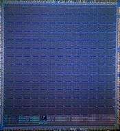
Asynchronous array of simple processors
The asynchronous array of simple processors (AsAP) architecture comprises a 2-D array of reduced complexity programmable processors with small scratchpad memories interconnected by a reconfigurable mesh network. AsAP was developed by researchers in the VLSI Computation Laboratory (VCL) at the University of California, Davis and achieves high performance and energy-efficiency, while using a relatively small circuit area.
AsAP processors are well suited for implementation in future fabrication technologies, and are clocked in a globally asynchronous locally synchronous (GALS) fashion. Individual oscillators fully halt (leakage only) in 9 cycles when there is no work to do, and restart at full speed in less than one cycle after work is available. The chip requires no crystal oscillators, phase-locked loops, delay-locked loops, global clock signal, or any global frequency or phase-related signals whatsoever.
The multi-processor architecture efficiently makes use of task-level parallelism in many complex DSP applications, and also efficiently computes many large tasks using fine-grained parallelism.
Key features

AsAP uses several novel key features, of which four are:
- Chip multi-processor (CMP) architecture designed to achieve high performance and low power for many DSP applications.
- Small memories and a simple architecture in each processor to achieve high energy efficiency.
- Globally asynchronous locally synchronous (GALS) clocking simplifies the clock design, greatly increases ease of scalability, and can be used to further reduce power dissipation.
- Inter-processor communication is performed by a nearest neighbor network to avoid long global wires and increase scalability to large arrays and in advanced fabrication technologies. Each processor can receive data from any two neighbors and send data to any combination of its four neighbors.
AsAP 1 chip: 36 processors

A chip containing 36 (6x6) programmable processors was taped-out in May 2005 in 0.18μm CMOS using a synthesized standard cell technology and is fully functional. Processors on the chip operate at clock rates from 520 MHz to 540 MHz at 1.8V and each processor dissipates 32 mW on average while executing applications at 475 MHz.
Most processors run at clock rates over 600 MHz at 2.0V, which makes AsAP among the highest known clock rate fabricated processors (programmable or non-programmable) ever designed in a university; it is the second highest known in published research papers.
At 0.9V, the average application power per processor is 2.4 mW at 116 MHz. Each processor occupies only 0.66mm².
AsAP 2 chip: 167 processors

A second generation 65 nm CMOS design contains 167 processors with dedicated fast Fourier transform (FFT), Viterbi decoder, and video motion estimation processors; 16 KB shared memories; and long-distance inter-processor interconnect. The programmable processors can individually and dynamically change their supply voltage and clock frequency. The chip is fully functional. Processors operate up to 1.2 GHz at 1.3 V which is believed to be the highest clock rate fabricated processor designed in any university. At 1.2 V, they operate at 1.07 GHz and 47 mW when 100% active. At 0.675 V, they operate at 66 MHz and 608 μW when 100% active. This operating point enables 1 trillion MAC or arithmetic logic unit (ALU) ops/sec with a power dissipation of only 9.2 watts. Due to its MIMD architecture and fine-grain clock oscillator stalling, this energy efficiency per operation is almost perfectly constant across widely varying workloads, which is not the case for many architectures.
Applications
The coding of many DSP and general tasks for AsAP has been completed. Mapped tasks include: filters, convolutional coders, interleavers, sorting, square root, CORDIC sin/cos/arcsin/arccos, matrix multiplication, pseudo random number generators, fast Fourier transforms (FFTs) of lengths 32-1024, a complete k=7 Viterbi decoder, a JPEG encoder, a complete fully compliant baseband processor for an IEEE 802.11a/g wireless LAN transmitter and receiver, and a complete CAVLC compression block for an H.264 encoder. Blocks plug directly together with no required modifications. Power, throughput, and area results are typically many times better than existing programmable DSP processors.
The architecture enables a clean separation between programming and inter-processor timing handled entirely by hardware. A recently finished C compiler and automatic mapping tool further simplify programming.
See also
References
- Truong, Dean; Wayne H. Cheng; Tinoosh Mohsenin; Zhiyi Yu; Anthony T. Jacobson; Gouri Landge; Michael J. Meeuwsen; Anh T. Tran; Zhibin Xiao; Eric W. Work; Jeremy W. Webb; Paul V. Mejia; Bevan M. Baas (April 2009). "A 167-Processor Computational Platform in 65 nm CMOS". IEEE Journal of Solid-State Circuits. 44 (4). Archived from the original on 2015-06-21.
- Truong, Dean; Cheng, Wayne; Mohsenin, Tinoosh; Yu, Zhiyi; Jacobson, Toney; Landge, Gouri; Meeuwsen, Michael; Watnik, Christine; Mejia, Paul; Tran, Anh; Webb, Jeremy; Work, Eric; Xiao, Zhibin; Baas, Bevan M. (June 2008). "A 167-processor 65 nm Computational Platform with Per-Processor Dynamic Supply Voltage and Dynamic Clock Frequency Scaling". In Proceedings of the IEEE Symposium on VLSI Circuits, 2008. Honolulu, HI. pp. 22–23. Archived from the original on 2014-12-25.
- Baas, Bevan; Yu, Zhiyi; Meeuwsen, Michael; Sattari, Omar; Apperson, Ryan; Work, Eric; Webb, Jeremy; Lai, Michael; Mohsenin, Tinoosh; Truong, Dean; Cheung, Jason (March–April 2007). "AsAP: A Fine-grain Multi-core Platform for DSP Applications". IEEE Micro. 27 (2). Archived from the original on 2015-06-25.
- Baas, Bevan; Yu, Zhiyi; Meeuwsen, Michael; Sattari, Omar; Apperson, Ryan; Work, Eric; Webb, Jeremy; Lai, Michael; Gurman, Daniel; Chen, Chi; Cheung, Jason; Truong, Dean; Mohsenin, Tinoosh (August 2006). "Hardware and Applications of AsAP: An Asynchronous Array of Simple Processors". In Proceedings of the IEEE HotChips Symposium on High-Performance Chips, (HotChips 2006). Stanford.
- Yu, Zhiyi; Meeuwsen, Michael; Apperson, Ryan; Sattari, Omar; Lai, Michael; Webb, Jeremy; Work, Eric; Mohsenin, Tinoosh; Singh, Mandeep; Baas, Bevan M. (February 2006). "An Asynchronous Array of Simple Processors for DSP Applications". In Proceedings of the IEEE International Solid-State Circuits Conference, (ISSCC '06). San Francisco, CA. pp. 428–429, 663. Archived from the original on 2014-12-25.
External links
- VLSI Computation Lab, UC Davis
- Asynchronous Array of Simple Processors (AsAP) project
- EETimes article describing AsAP