Phase-shift mask


Phase-shift masks are photomasks that take advantage of the interference generated by phase differences to improve image resolution in photolithography. There exist alternating[1] and attenuated phase shift masks.[2]
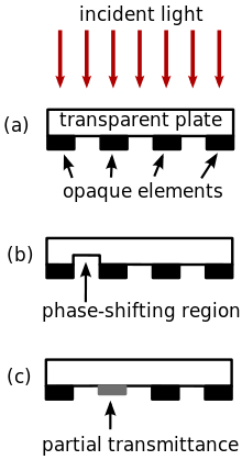
A conventional photomask is a transparent plate with the same thickness everywhere, parts of which are covered with non-transmitting material in order to create a pattern on the semiconductor wafer when illuminated.
In alternating phase-shift masks, certain transmitting regions are made thinner or thicker. That induces a phase-shift in the light traveling through those regions of the mask (see the illustration on the left). When the thickness is suitably chosen, the interference of the phase-shifted light with the light coming from unmodified regions of the mask has the effect of improving the contrast on some parts of the wafer, which may ultimately increase the resolution on the wafer. The ideal case is a phase shift of 180 degrees, which results in all the incident light being scattered. However, even for smaller phase shifts, the amount of scattering is not negligible. It can be shown that only for phase shifts of 37 degrees or less will a phase edge scatter 10% or less of the incident light.
Attenuated phase-shift masks employ a different approach. Certain light-blocking parts of the mask are modified to allow a small amount of light to be transmitted through (typically just a few percent). That light is not strong enough to create a pattern on the wafer, but it can interfere with the light coming from the transparent parts of the mask, with the goal again of improving the contrast on the wafer.
Attenuated phase-shift masks are already extensively used, due to their simpler construction and operation, particularly in combination with optimized illumination for memory patterns. On the other hand, alternating phase-shift masks are more difficult to manufacture and this has slowed their adoption, but their use is becoming more widespread. For example, the alternating phase-shift mask technique is being used by Intel to print gates for their 65 nm and subsequent node transistors.[3][4] While alternating phase-shift masks are a stronger form of resolution enhancement than attenuated phase-shift masks, their use has more complex consequences. For example, a 180 degree phase edge or boundary will generally print. This printed edge is usually an unwanted feature and is usually removed by a second exposure.
A benefit of using phase-shift masks in lithography is the reduced sensitivity to variations of feature sizes on the mask itself. This is most commonly used in alternating phase-shift masks, where the linewidth becomes less and less sensitive to the chrome width on the mask, as the chrome width decreases. In fact, even with no chrome the phase edge can still print, as noted above. Some cases of attenuated phase-shifting masks also demonstrate the same benefit (see left).
As phase-shift masks are applied to printing smaller and smaller features, it becomes more and more important to model them accurately using rigorous simulation software, such as Panoramic Technology or Sigma-C. It becomes especially important as the mask topography starts to play an important role in scattering the light, and the light itself starts to propagate at larger angles. The performance of phase-shift masks can also be previewed with the use of aerial image microscopes. Defect inspection remains a critical aspect of phase-shift mask technology, as the set of printable mask defects has expanded to include those with phase effects in addition to conventional transmission effects.
References
- ↑ "Alternating phase shift masks at FreePatentsOnline".
- ↑ "Attenuated phase shift masks at FreePatentsOnline".
- ↑ A. Tritchkov, S. Jeong, and C. Kenyon, "Lithography Enabling for the 65 nm node gate layer patterning with Alternating PSM," Proc. SPIE vol. 5754, pp.215-225 (2005).
- ↑ S. Perlitz et al., "Novel solution for in-die phase control under scanner equivalent optical settings for 45-nm node and below," Proc. SPIE vol. 6607 (2007).
Further reading
- Levinson, Harry (2004). Principles of Lithography (2nd ed.). SPIE—The International Society for Optical Engineering. ISBN 0-8194-5660-8.
- Rai-Choudhury, P., editor (1997). Handbook of Microlithography, Micromachining, and Microfabrication. Volume 1: Microlithography. Bellingham, Washington: SPIE Optical Engineering Press. ISBN 0-85296-906-6.